Crack Examination in Electronic Components
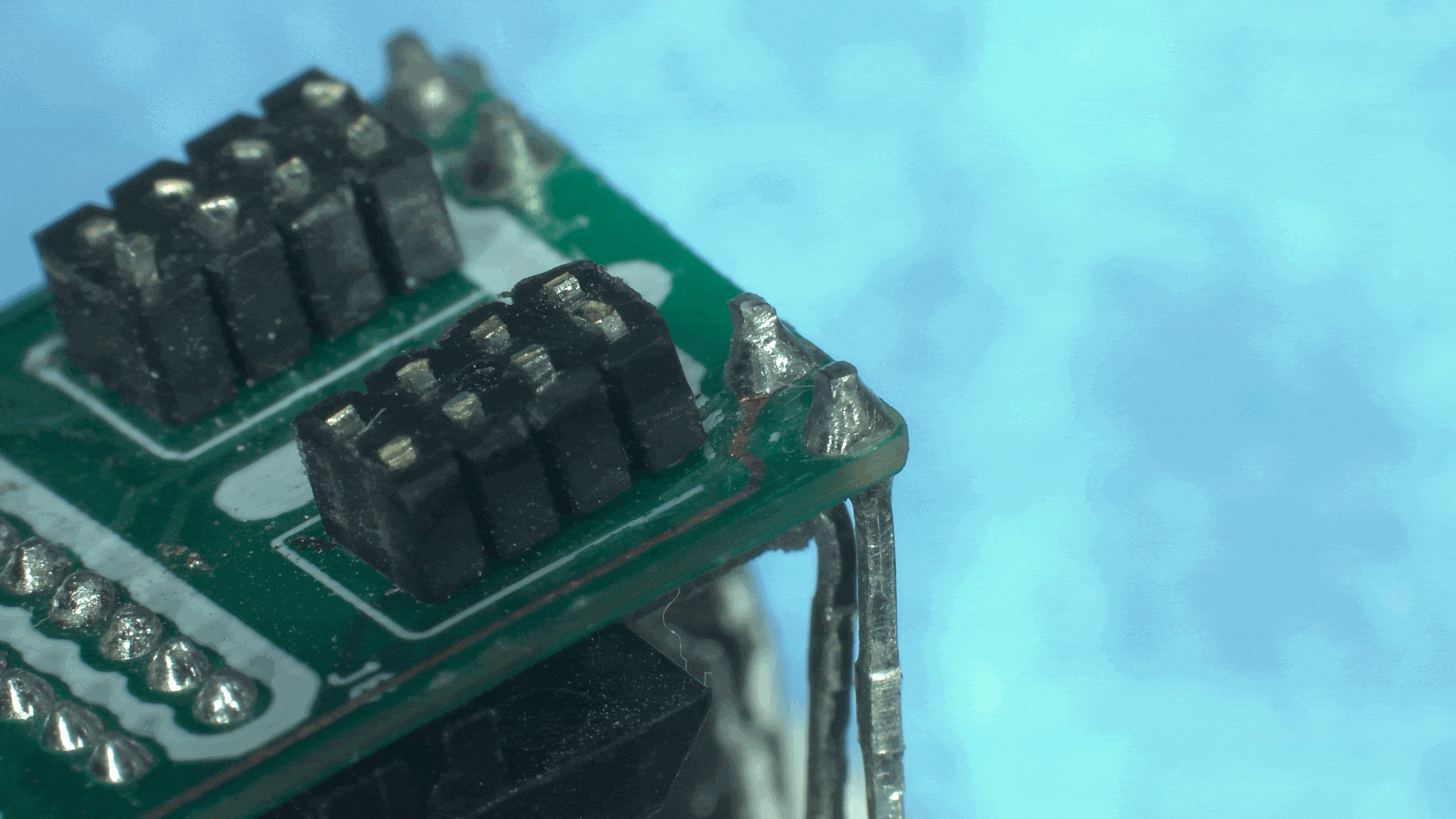
One case I was involved in related to a break in a circuitry board. I was contacted by an Irish-based multinational corporation, who produce bespoke electronic goods for specific communication applications. One particular critical component was found to be having intermittent failures on a specific LED bulb. They sent the component assembly to me, and I began my investigation.
Firstly, the component assembly had to be disassembled, to expose the LED causing issues for an initial microscopy analysis. This involved a mixture of mechanical unfastening, and precision cutting. Once freed, I examined LED, it’s legs, and the connection to the circuit board. What was initially invisible to the naked eye quickly became apparent. There was a small crack between the copper track running through the circuit board, and the plated landing where the LED leg was soldered in.

Wanting to examine this crack further, and attempt to measure the size of the crack, I encased the component in epoxy resin. Because of the free-standing LED legs, I used a vacuum impregnation device to pull the air out from around the component, and replace it with slow cure epoxy. Once this mounting process was complete, I used grinder/polisher metallography equipment to slowly abrade through the circuit board, to expose the board side-on.

Examining this cross-section of the component shows the crack as clear as day, and allowed me to measure the size of the crack at less than 9 micrometers, smaller than the average human hair!
The elemental composition of the copper and the solder was measured, and found to be normal. Ultimately, the crack was attributed to the movement induced stresses from the environment.
Microscopy is an extraordinarily powerful tool in the analysis of electronic components, and the addition of metallographic techniques brings the examination to the next level. If you think microscopy can help resolve your issue, then contact me today!